Materials Used in PCBs
The composition of printed circuit boards (PCBs) is crucial to their functionality. Typically, they are constructed from materials that can withstand various environmental conditions while ensuring electrical conductivity. Common substrates include fiberglass-epoxy composites, such as FR-4, which provide durability and insulation. Other materials used for flexibility include polyimides, suitable for applications requiring bendability. The choice of substrate often reflects the specific demands of the application, whether in consumer electronics or industrial machinery.
Conductive materials play a vital role in PCB design and performance. Copper is the most widely used metal for traces due to its excellent conductivity. Thinner layers can be employed to achieve precise circuit patterns, often supported by processes like electroplating or etching. Other metals, such as aluminum or gold, may be used in specialized applications for enhanced performance, particularly where corrosion resistance is a key concern. Overall, the selection of both substrate and conductive materials is integral to meeting the operational requirements of modern electronic devices.
Common Substrates and Conductive Materials
The choice of substrate material in PCB design significantly influences performance and durability. Fiberglass-reinforced epoxy (FR4) is the most prevalent substrate, offering a balance of strength, electrical insulation, and thermal stability. Other materials like polyimide are utilized for high-temperature applications, while specialty substrates are available for specific needs. Each option has its own set of features that cater to different operational requirements.
Conductive materials primarily used in PCBs include copper and aluminum. Copper is the standard choice due to its excellent conductivity and ease of processing, often employed in various thicknesses depending on current requirements. Aluminum, while less common, is used in applications that demand lightweight characteristics or enhanced thermal dissipation. The selection of conductive materials is crucial for optimizing electrical performance and overall circuit efficiency.
Advantages of Using PCBs
Printed circuit boards (PCBs) offer numerous advantages in electronic design and manufacturing. They provide a compact and organized layout for electronic components, which optimizes space and facilitates effective electrical connections. This design minimizes wiring errors and enhances the overall reliability of the circuit. Moreover, PCBs can handle a large number of connections, making them ideal for complex electronic devices where space and efficiency are critical.
The durability of PCBs contributes significantly to their widespread use. Constructed from robust materials, they can withstand varying environmental conditions, from temperature fluctuations to moisture. This resilience ensures that devices remain functional over extended periods, reducing the need for frequent repairs or replacements. Additionally, the automated manufacturing processes used for PCBs promote consistency and quality, leading to lower production costs in mass manufacturing.
Efficiency and Reliability in Circuitry
The construction of printed circuit boards (PCBs) enhances electrical efficiency by providing a structured platform for components. Precise routing of electrical paths minimizes resistance, which results in lower energy losses. Additionally, a well-designed PCB can support high-frequency signals with minimal signal degradation, making it suitable for a variety of applications from consumer electronics to industrial machinery.
Reliability in PCB design stems from the use of durable materials and robust manufacturing processes. Quality control measures ensure that each board meets strict performance standards, reducing the likelihood of failure in critical applications. With advancements in technology, such as multi-layer boards and embedded passive components, manufacturers achieve greater reliability while maintaining compact designs to fit modern requirements. This focus on durability is essential for industries where downtime can result in significant financial loss.
Challenges in PCB Manufacturing
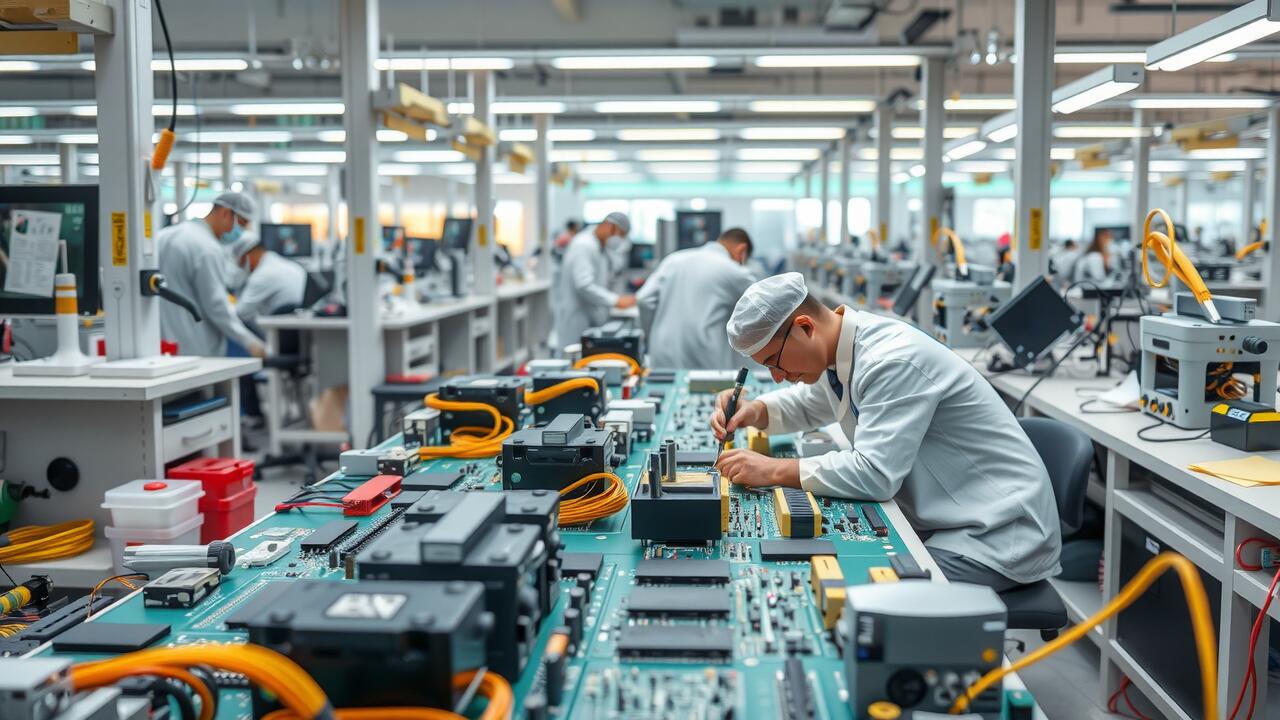
The process of PCB manufacturing is fraught with various challenges that can affect both production time and the overall quality of the final product. One significant issue is achieving proper alignment during the layering process. Misalignment can lead to faulty connections, which may compromise the functionality of the circuit. Additionally, maintaining clean manufacturing environments is crucial. Contaminants such as dust or humidity can interfere with the adhesion of solder masks and inks, resulting in unreliable performance.
Another challenge is the increasing complexity of designs, which often requires higher precision in both layout and production techniques. As electronic devices become more advanced, the demand for finer traces and smaller component footprints grows. Meeting these specifications can strain the capabilities of existing machinery. Furthermore, the ever-evolving technology landscape necessitates continuous training of staff to handle new materials and processes effectively. Addressing these issues is essential for staying competitive in the fast-paced electronics sector.
Common Issues and Solutions
In the realm of PCB manufacturing, several issues can arise that may compromise the production process or the integrity of the final product. One common challenge is the misalignment of layers during the lamination process, leading to shorts or opens in circuits. Operators must ensure precise registration of layers to mitigate this issue. Additionally, delamination can occur due to various factors, including improper curing or moisture absorption. Close monitoring of environmental conditions during curing and careful material selection can address these concerns effectively.
Another prevalent issue is the occurrence of solder bridging, which can happen during the soldering process, especially when component pitches are tight. This defect can short circuit connections, leading to failures in the final assembly. Implementing stricter process controls and adjustments in the solder paste application can help reduce this risk. Furthermore, inadequate surface finish can result in poor solderability, necessitating thorough inspections and appropriate surface treatment processes to enhance adhesion and overall reliability.
FAQS
What is a PCB?
A PCB, or Printed Circuit Board, is a flat board that electrically connects and supports electronic components using conductive pathways, tracks, or pads made from copper.
What are the primary uses of PCBs?
PCBs are primarily used in electronic devices to provide structural support for components, facilitate electrical connections, and ensure efficient circuitry for various applications such as computers, smartphones, and appliances.
What materials are commonly used in PCB manufacturing?
Common materials used in PCB manufacturing include substrates like FR-4 (a fiberglass epoxy), various types of copper for conductive pathways, and solder masks for protecting the circuitry.
What advantages do PCBs offer over other circuit construction methods?
PCBs offer several advantages, including improved efficiency and reliability in circuitry, reduced size and weight of electronic devices, and enhanced durability and resistance to environmental factors.
What are some common challenges faced in PCB manufacturing?
Common challenges in PCB manufacturing include issues such as signal integrity, thermal management, and manufacturing defects. Solutions often involve advanced design techniques and quality control processes to mitigate these problems.