Component Placement
Effective component placement is crucial for ensuring optimal performance and reliability in PCB design. Start by considering the electrical and thermal characteristics of each component. Position sensitive components away from high-heat areas and ensure that high-frequency signals can travel with minimal interference. Utilizing a grid system can help maintain uniform distances between components and improve overall layout efficiency.
It is also important to prioritize accessibility during the assembly and troubleshooting phases. Components should be spaced adequately to allow for soldering and inspection. Grouping similar components can streamline the manufacturing process and reduce potential errors. Careful planning during this stage translates into a more efficient assembly workflow and enhances the longevity of the final product.
Strategies for Effective Layout
Effective PCB layout starts with a clear understanding of the circuit's functionality and signal flow. Arranging components in a logical order helps minimize trace lengths, reducing potential interference and signal degradation. Placing components close to each other, especially those that interact frequently, can streamline connections. Additionally, grouping similar components such as power supply parts together can simplify routing and enhance thermal management.
Consideration for component orientation is also essential. Aligning components consistently helps in maintaining visual clarity and eases soldering. Utilizing a grid layout can enhance organization, allowing smoother transitions between traces. Prioritize placing larger components first to establish a framework, then fill in smaller components around them. This method creates a more efficient layout, facilitating easier debugging and assembly.
Soldering Techniques
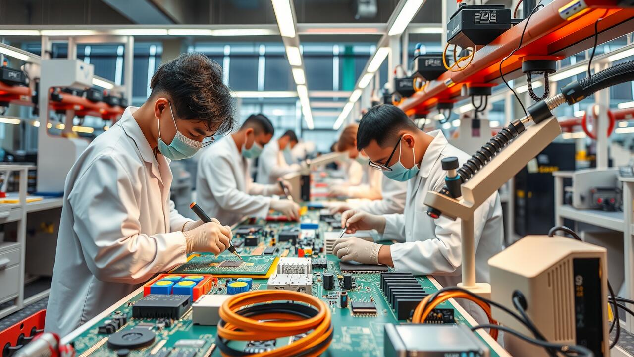
Soldering is the process of joining electronic components to a printed circuit board (PCB) using a metal alloy known as solder. This technique requires careful temperature control to ensure proper adhesion without damaging sensitive components. The choice of solder, such as leaded or lead-free options, can affect both the ease of soldering and the longevity of the connections. Proper preparation of the pads and leads, along with the use of appropriate tools like soldering irons or hot air rework stations, is essential for achieving strong joints.
Different soldering techniques can be employed depending on the complexity of the assembly and the component types being used. Wave soldering is often utilized for through-hole components in high-volume productions, while surface mount technology (SMT) may benefit from reflow soldering. For hobbyists or in small-scale projects, hand soldering remains the most accessible method. Each technique comes with its own set of best practices to ensure effective solder joints that can withstand the rigors of electrical use and thermal cycling.
Methods for Joining Components
The most common method for joining electronic components to a PCB is through soldering. This technique involves melting solder, typically made of tin and lead or lead-free alternatives, to create a reliable electrical connection. Soldering can be performed using various methods, including hand soldering with a soldering iron and reflow soldering, which is often employed in mass production settings such as surface mount technology (SMT). When applying solder, it is crucial to achieve an optimal joint. This requires the right amount of heat and time to ensure proper adhesion without damaging components or the PCB itself.
Another popular technique for joining components is using adhesives or conductive epoxies. These materials can be especially valuable in specific applications where traditional soldering may not be suitable, such as when working with heat-sensitive components or in environments prone to mechanical stress. Adhesives can create strong bonds and provide electrical connectivity between components and the board. Proper surface preparation is vital for achieving a strong joint with adhesives, involving cleaning the surfaces and ensuring adequate curing time for maximum strength. Each method requires careful consideration of the materials and components involved to ensure a successful assembly.
Testing the Assembly
After the assembly process, thorough testing is crucial to ensure the circuit operates as intended. A visual inspection using magnification tools can help identify any solder bridges, misaligned components, or cold solder joints. This initial step often saves time by addressing potential issues before deeper testing begins. Following this inspection, a multimeter is typically employed to check for continuity in the circuit connections. This ensures that all the paths are correctly established and ready for power application.
Once basic continuity is confirmed, applying power to the circuit becomes the next step. Monitoring voltage levels at various points can help identify discrepancies that might point to defects or faults in the design. Utilizing an oscilloscope may be advantageous for more complex circuits, allowing for observation of waveforms and signal integrity. Running functional tests based on the circuit’s intended purpose also verifies that it meets performance specifications and behaves as expected under operational conditions.
Ensuring Circuit Functionality
Testing the assembled PCB is a crucial step in the production process. This ensures that the circuit functions as intended. Various methods can be employed, such as using a multimeter to check continuity and measure voltage levels across different points on the board. Additionally, employing oscilloscopes can help visualize signals, confirming that they align with design specifications.
Functional testing involves running the board under its intended operational conditions. This can reveal any discrepancies or faults that may not have surfaced during earlier testing phases. Utilizing test fixtures or software can streamline this process. Properly identifying and addressing issues will ultimately lead to a reliable and efficient final product.
FAQS
What is the first step in assembling a PCB?
The first step in assembling a PCB is component placement, where you strategically position all electronic components on the board according to the design layout.
How can I effectively layout components on a PCB?
Effective layout strategies include grouping similar components together, maintaining adequate spacing for soldering, and considering heat dissipation to avoid interference between components.
What are the common soldering techniques used in PCB assembly?
Common soldering techniques include hand soldering, reflow soldering, and wave soldering, each suited for different assembly scales and types of components.
How do I ensure my soldered components are joined properly?
To ensure proper joining of components, you should use the right amount of solder, heat the joint adequately, and visually inspect connections for any cold solder joints or bridges.
What tests should I perform after assembling a PCB?
After assembly, you should conduct continuity tests, inspect for solder quality, and perform functional tests to ensure the circuit operates as intended.